集成电路
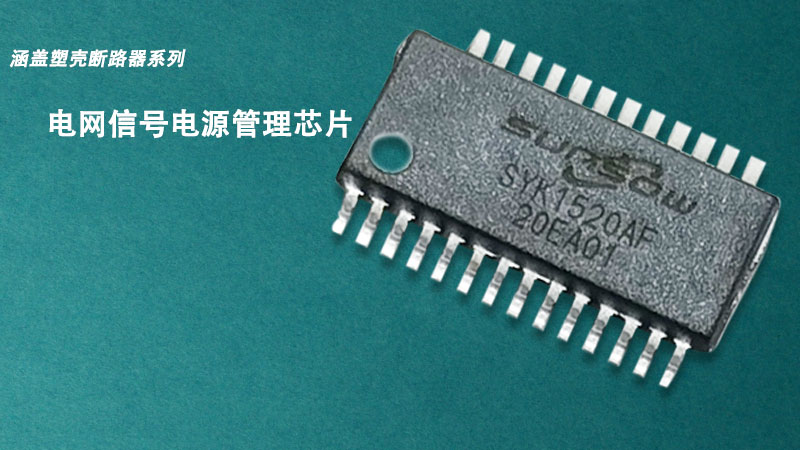
SYK1520AF电网信号电源管理芯片
该芯片是一款针对低压电器的需求而研制,行业内率先开发的集多功能于一体的专用芯片;属于国内首创的电网信号与电源管理控制专用芯片,相比原来由分立器件来实现功能的电路,解决多项技术瓶颈。
• 全新自主架构,与之配合的外围电路极其简单,无需额外的供电电路。
• 采用新型的电压校正技术,通道失调电压小于1mV。
• 1A的脱扣电流和纳秒级响应速度,确保脱扣保护快速可靠,兼容双驱动脱扣线圈。
• 完善的过温、过流、过压欠压等保护功能,确保芯片可靠稳定。
• 采用先进的40V BCD工艺,器件耐压远高于工作电压,确保充分的工作电压裕量。
主要应用领域:低压电器,国家电网,智能家居,能效管理。
General Description
The SYK1520AF is a special controller for power management, power grid signal detection and protection switch. It mainly includes four parts. The first part is the power management, which supplies energy to the controller through the signalisolator, and the built-in power supply voltage detection circuit ensures that the power supply voltage of the controller is stable at 12Vdc/9Vdc, when the power supply voltage exceeds the internal comparison voltage, the DRV pin will output high level to drive the external NMOSFET on to form a current discharge path. The second part is the external output power supply, and the built-in LDO is used to generate 5Vdc/3.3Vdc regulated power supply, with the maximum current capacity of 200mA. The third part is protection switch, the built-in current driving capacity of open drain output MOSFET is 500mA, which is used to drive the tripping coil and provide fast tripping response to improve the system reliability. The fourth part is the signal detection, with built-in high-accuracy and low-power consumption differential operational amplifier, the gain of the first to the fourth operational amplifier is fixed, and the gain of the fifth operational amplifier is adjustable.
Features
● Five-channel high-accuracy and low-power consumption operational amplifier, rail to rail output
● The gain of four-channel operational amplifier is fixed, the gain of one-channel operational amplifier is adjustable
● 3.3Vdc/5.5Vdc high-accuracy LDO, the output current is 200mA
● Built-in voltage detection circuit to stabilize the supply voltage at 12Vdc/9Vdc
● Built-in open drain MOSFET to drive the tripping coil
● Over temperature protection
● Over current protection
● Over voltage protection and under voltage protection
● ETSSOP-28 Package
Applications
● Low voltage circuit breaker
● CT current transformer power supply
Simplified Application

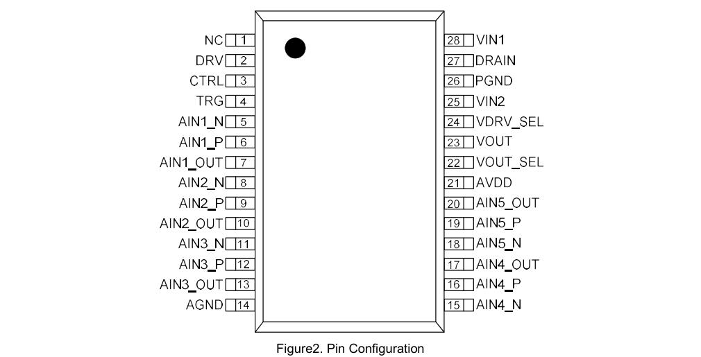
Pin Function Description


Ordering and Marking Information

Absolute Maximum Ratings

Note:
Note 1. Stresses listed as the above “Absolute Maximum Ratings” may cause permanent damage to the device. These are for stress ratings. Functional operation of the device at these or any other conditions beyond those indicated in the operational sections of the specifications is not implied. Exposure to absolute maximum rating conditions for extended periods may remain possibility to affect device reliability.
Block Diagram


Electrical Characteristics
VIN =12V, T A = +25°C, unless otherwise specified


Typical application diagram


Typical Characteristics
TA = +25°C, unless otherwise specified


Functional Description
The energy of SYK1520AF is provided by the isolator, which monitors the voltage change of VIN1 in real time to control the external NMOSFET on and off. When the voltage of VIN1 is higher than the internal clamping voltage, the voltage of DRV changes from low to high to control the external NMOSFET on, and the isolator stops providing energy to the controller, and then the external capacitor provides energy for the back-end load. When the voltage of VIN1 is lower than the comparative hysteresis voltage, the voltage of DRV changes from high to low level to control the external NMOSFET off, and the isolator starts providing energy to the controller.
Clamping voltage selection
When VDRV_SEL is low level, the voltage of VIN1 is clamped to 12Vdc, and the hysteresis voltage is 0.3Vdc.
When VDRV_SEL is high level, the voltage of VIN1 is clamped to 9Vdc, and the hysteresis voltage is 0.25Vdc.
Output power supply
The external power supply input VIN2 can be connected to VIN1 pin through an external resistance, which is used
to consume part of the power consumption to reduce the internal power consumption of the controller. The VOUT
pin of the controller needs to be connected with a 1μF capacitor to the ground to ensure the stability of the power
loop. The output voltage of the internal regulated power supply is 3.3Vdc/5Vdc, and the limit current is 250mA to
ensure the stability of the subsequent power supply.
Operational amplifier power supply
The power supply pin of the internal operational amplifier is AVDD pin, which needs to be connected to VOUT pin.
Output voltage selection When VOUT_SEL is low level, the output voltage of the controller is 3.3Vdc. When VOUT_SEL is high level, the output voltage of the controller is 5Vdc.
Under voltage protection
When the voltage of VIN1 is higher than 6V, the controller will start operation; when the voltage of VIN1 is lower than
5.3V, the controller turns off the power supply, that is, theVOUT voltage turns off.
Over temperature protection
SYK1520AF is internally integrated with over temperature protection function. The DRAIN pin will be pulled down to
control the trip action when the temperature of the controller exceeds 150℃. When the temperature of the
controller is lower than 115℃, the controller will resume normal operation.
Control function of TRG
The DRAIN pin will be pulled down to control the trip action when the voltage of TRG is high level. In normal
operation, TRG is low.
Control function of CTRL
The DRV will output high level to drive the external NMOSFET on when CTRL is high level, and the isolator
stops supplying power to the controller. In normal operation, the CTRL is low.
High-accuracy and low-power consumption operational amplifier
SYK1520AF is internally integrated with five-channel rail to rail operational amplifiers, the gain of the first to fourth
operational amplifier is fixed at 1, and the gain of the fifth operational amplifier is externally adjustable.
Package Information(Units: mm)


